Power Supply For Students

Power Supply For Students | Design Your Own Power Supply | Regulated Power Supply Design

My First Project As A Student Of Electronics Engineering - Design Power Supply

When I was a student of Electronics engineering, this was the first task, that is to design a power supply unit. It might be your first project during the first semester of ECE discipline as well. We are going to design a variable power supply with a maximum output voltage of 24V.

Project Goals & Outline:
  • What is a power supply unit and why it is important?
  • Block diagram and explain each block
  • Circuit diagram and explanation of each component
  • Choosing the right components
  • Specifically designed calculators, which help in selecting the right capacitance and resistance

After thoroughly reading this lesson you will be able to design a regulated and variable power supply of desired value. I have designed my calculator, you can calculate the value of the capacitor (filtering or smoothing capacitor), and resistors values (for LM317) according to your need. You can able to select the right components, as I discuss which component is suitable for this purpose.

What is PSU (Power Supply Unit):

A power supply is nothing but a unit for conversion of available AC to DC voltage. The conversion of AC to DC is one of the fundamental concepts of electronics. The circuit consists of basic components like diodes, capacitors and a capacitor. In this post, we have to design a regulated power supply, so we add a regulator IC (i am going to use LM317).

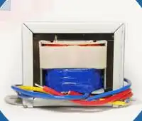
Choosing the right transformer for step-down AC voltage:

Here the purpose of the transformer is to step down the available AC voltage. You get AC voltage from your socket which is equal to 240V or 120V.

How do you choose the right transformer?
I am not going into the details of the transformer. Transformers have standard ratings. You can not build a transformer of your own choice. It is the art to choose the right transformer. As a beginner, it is quite difficult for you to choose the right transformer. Please carefully read my guide, it may help you. 

First of all, decide what would be the output voltage of your power supply. In my case, I decide to make it 20V. It can regulate voltage from 0 to 20V. There are transformers available, which can step down output 24V AC. (Other ratings are 12V, 18V etc). The output of the transformer depends on its primary to secondary turns ratio.
You can calculate the estimated output by using this formula,
NP/NS = VP/VS
Where
NP = Number of primary winding turns
NS = Number of secondary winding turns
VP = Voltage at primary windings
VS  =Voltage at secondary windings
With the help of this formula, you can calculate the primary to secondary turns ratio (NP/NS)

Example#1: Evaluate NP/NS ratio, when incoming AC voltage is 120V, and step down up to 20V
VP = 120V
VS = 20V
NP/NS = 6

Example#2: Evaluate NP/NS ratio, when incoming AC voltage is 240V, and step down up to 24V
VP = 240V
VS = 24V
NP/NS = 10

                
Please handle it with care, you can get an electric shock. Please first use any relevant CAD software, to design your project, then come to hardware components.


Basic power supply circuit
Power Supply - Schematic diagram and block diagram

The rectification process for AC to DC conversion:
This block performs two tasks. The first is rectification. After rectification, the output is fed to a smoothing or filtering capacitor. We will first discuss the bridge rectifier and then the smoothing capacitor.

Needless to explain rectifier block, as is already discussed in detail here. This is the heart of the whole system. It consists of four diodes, which convert AC to pulsating DC. Bridge rectifier IC is available, however, you can use four discrete diodes as well. GBJ2510 is a bridge rectifier IC.


  • You get 24V from secondary windings of the transformer
  • After rectification, you get pulses, with a peak value of 22.6V
  • We consider diode drop which is equal to (0.7+0.7)V
  • We have to eliminate the pulses, so let's come to the next part of this block

While designing your circuit, you might confuse about component selection. You can use discrete diodes for this purpose. But it is recommended to use a bridge rectifier IC. There are bridge rectifier IC available in the market.
MCIGICM 25A 1000V diode bridge rectifier gbj2510

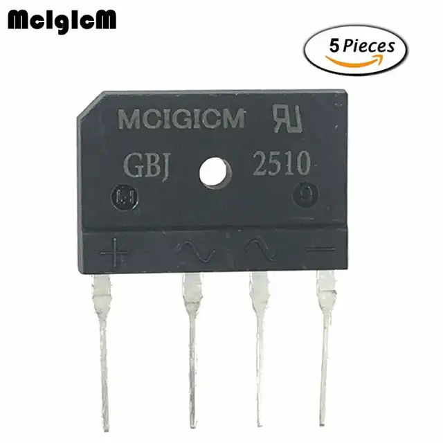
What does a bridge rectifier IC look like?
Specifications of GBJ2510

This block also contains a capacitor. The capacitor smoothes the pulsating DC voltage. This is the smoothing capacitor or filtering capacitor. To get ripple-free voltage, you need to select a proper capacitance value. The discharging time of the capacitor should be high.
Choosing a smoothing capacitor is also a little bit tricky.
  • The first time you might have rippled output, but don't worry
  • You just have to adjust the capacitor value, once you get the appropriate capacitor, you get the smooth DC

I discussed this equation in a full-wave rectifier. The equation is helpful for the evaluation of the capacitance value.
Note: the above formula is only valid if the ripple voltage value is not more than 20% of the peak voltage.

I designed a calculator, input appropriate values, you get the desired value of the capacitor.


Volt
Volt
Ohm
Hertz
farad


The Regulator Block:
The voltage regulator maintains a constant voltage level at the output irrespective of no load or full load condition. This block is added in between input and output. It resists any change in input voltage and output load and maintains a constant voltage.
We are using LM317 as a positive voltage regulator. Its specifications are
  • Adjustable output voltage ranges from 1.25V to 37V
  • Input voltage ranges from 3 to 40V
  • Output current 1.5A

Look it is a three-terminal device. As a beginner, you can easily use it in your circuit.
LM317 Regulator IC


How do we connect it to the circuit…?

Look at the regulator block. It consists of LM317, two resistors (R1 and R2) and two capacitors (C2 and C3). The capacitors are decoupling capacitors. The resistors make a voltage divider circuit. With the help of these resistors, we can adjust the output.
Designers recommend it is better to set R1 = 240,
There is a targeted output voltage Vout, which is equal to 20V in this case. With the help of the given formula, you can calculate R2.
Here is a calculator, you have to enter any two variables, and it will evaluate the third one.
Ohm
Ohm
Volt

Conclusion:

I hope you understand the working and operation of the power supply circuit. It is one of the basic circuits. You can find a variety of circuits. If you would able to properly design your power supply unit, then this will power your electronic projects in future.
Ohm
Ohm
Volt

Diode Approximations | Diode Models

Diode Approximations | Diode Models
You might come across the terms ideal and practical diodes. As a beginner, these terms might confuse you. So, I think it is important to discuss the properties of an ideal diode and a practical diode.

Outline
  • Discuss different diode approximation or diode models
  • How does practical and ideal diode model differ from each other?
  • Why do we need to learn the behaviour of an ideal diode?

Diode Models And IV Characteristics:

The current-voltage characteristics curve is shown in figure 7. Look at the graph, how much a practical diode deviates from ideal behaviour. An ideal diode is a piecewise linear device, while a practical diode is a non-linear device. Linear device means its current-voltage graph is a straight line. A diode is non-linear because its current-voltage graph is a non-linear curve. For voltage values less than 0.7V, the current is zero. Just above 0.7V, the current increases rapidly. Current doesn't increase proportionally to an increase in voltage.

First Approximation Or Ideal diode:

This is the simplest approximation. The graph is simple and piecewise linear. Zero resistance when forward biased, infinite resistance when reverse biased. It is analogous to a mechanical switch. Because the switch has zero resistance when close. And a switch has infinite resistance when open. The voltage across the diode is 
VD = 0

Ideal diode in forward and reverse biased mode
Figure 1 Ideal diode and its equivalent

Diode first Approximation, IV Curve of ideal diode
Figure 2: Ideal diode IV Curve

Second Approximation Or Practical diode Model:

The graph is piecewise linear. Look at the graph, the diode doesn't conduct until the voltage reaches 0.7.

According to this approximation, a diode is analogous to a switch in series with a barrier potential of 0.7V. Look at the figure, the diode becomes forward bias when the applied potential is at least 0.7V (close switch). Hence current increase rapidly.
For applied voltage below 0.7V, it remains reverse bias (open switch). The voltage across the diode is
VD = 0.7 V

Diode second approximation and its equivalent
Figure 3 Non-ideal diode and its equivalent
Second approximation of diode - IV Curve
Figure 4 Non-ideal diode, IV Curve

Third Approximation Or Detailed Model:

According to this approximation, a diode is analogous to a switch, a barrier potential and a resistor (Rf), connected serially. Rf shows the internal resistance of semiconductors.

Now examine the effect of Rf. The diode turns on as the applied voltage is 0.7V or above. Thereafter, the current increases as an increase in voltage (Rf is ohmic resistance). We can apply Ohm's law and find voltage and current through it. The voltage across the diode is
VD = IDRf +0.7


Where
VD = diode voltage
ID = diode current
Rf = forward resistance of diode or bulk resistance

Third Approximation of diode and it's equivalent
Figure 5 Third approximation of diode
Diode IV Curve (a practical diode IV Curve)
Figure 6 Third approximation IV Curve

Difference between ideal and practical diode:

Compare IV curves of a practical and ideal diode
Figure 7 Practical diode Vs Ideal diode IV Curve

You have seen all three diode approximations. The figure above is the graph obtained from a real diode. In this graph, we consider all the effects of ohmic resistance, threshold voltage, leakage current and breakdown region.

Forward Biased

Ideal Diode
  • It behaves as a perfect conductor
  • An ideal diode is like a closed switch. It has 0Ω resistance between anode and cathode
  • No need for threshold voltage
  • It has zero resistance, and hence infinite current through the diode. (I = V/R)
Real Diode
  • It also acts as a conductor. Due to imperfections, it offers a small forward resistance Rf
  • It is also like a closed switch, except a small forward resistance Rf
  • Real diodes need a little voltage called knee voltage or threshold voltage to overcome barrier potential
  • Due to small forward resistance Rf, there is a voltage drop at the diode and hence finite current through the diode

Reverse Biased

Ideal Diode:
  • It behaves as a perfect insulator
  • An ideal diode is like an open switch in reverse bias conditions. No current can flow from anode to cathode
  • Breakdown region is not possible at any magnitude of applied voltage
Real Diode:
  • It behaves as an insulator. There is a voltage limit called the breakdown voltage. The diode can not operate beyond this limit
  • Real diodes deviate from ideal behaviour because of minority carriers. Due to minority carriers, it has some reverse current flows from cathode to anode. This current is called reverse saturation current or leakage current
  • They do have a breakdown voltage. If the applied voltage exceeds the rated voltage, results in junction breakdown

Need of Ideal Diode Behaviour:

You have read the features of an ideal diode. An ideal diode can not possible to produce. It has infinite resistance in reverse biased conditions, and hence no current. It has zero resistance in forwarding biased conditions, and hence infinite current. Such conditions are not possible practically.

Which diode model commonly use during analysis?
Most of the time we consider the third approximation.

Why do we consider an ideal diode?
We consider the ideal diode at the first stage of our analysis and troubleshooting. It is easy to understand the circuit analysis with an ideal diode. As a beginner, it is better to start with ideal diodes, to keep circuit analysis as simple as possible.


Biased & Unbiased Diode Clampers, Circuit Diagrams & Working

Biased And Unbiased Diode Clampers, Circuit Diagrams And Working

Applications of Diode - Types of Diode Clampers (Positive and Negative clampers, Biased and Unbiased Clampers) - Circuit Diagrams and Working, Waveforms and Comparison 

Another popular diode-based circuit is the clamping circuit. A clamper circuit or network adds DC level to a given AC signal without any change in signal shape. A simple circuit is shown below, comprise of a capacitor, diode and resistor. Carefully choose the capacitance value. The time constant should be large enough to maintain the shape of the output signal. The time constant can be increased by using larger capacitance values. Throughout this article, I consider a practical diode with a drop of 0.7V.

V1 is the sinusoidal input
VP is the peak voltage
Vo is the output voltage


Outline:
In this article, I explain different types of clamper circuits, like biased clampers and unbiased clampers, positive and negative clampers.

Comparison between biased positive clampers and unbiased positive clampers. 

Comparison between biased negative clampers and unbiased negative clampers.


Positive Clamper Circuit Diagram and Working:

It clamps the incoming signal to an upward direction. See the circuit below (figure 1). The diode arrow points upward. It means the signal is going to shift in an upward direction.

During the negative half-cycle, the diode turns on. As a result, the capacitor charges up to peak value (VP - 0.7V) that is 9.3V. (Considering practical diode)

During the positive half cycle, the diode opens (reverse bias). No path to flow current. To determine the output voltage that appears across the resistor, apply KVL to the loop.

Vo =  V1 + VP

Unbiased positive diode clamper circuit diagram
Figure 1 Positive Clampers, capacitance value should high to keep time constant large

Negative Clamper Circuit Diagram and Working:

It clamps the incoming signal to a downward direction. See the circuit below (figure 2). The diode arrow points downward. It means the signal is going to shift in a downward direction. Each point on the sine wave is shifted to a downward direction by an amount of VP.

During the positive half cycle, the diode turns on. As a result, the capacitor charges up to peak value (VP) which is 9.3 V (considering diode drop).

During the negative half-cycle, the diode opens (reverse biased). To determine the output voltage that appears across the resistor, apply KVL to the loop.

Vo = - Vi - VP
Unbiased diode negative clampers circuit diagram, working and waveforms
Figure 2 Negative Clampers

Positive Biased Clamper Circuit Working:

During the negative half-cycle, the diode is reverse biased for a small part of the input signal. This is because of DC source polarity (V2 = 2V). The anode is more positive than the cathode for a small part of the input waveform (V1 <V2). For higher values of V1 (V1> 2V) the diode turns on and capacitor charges with the polarity shown.
V1 - VC1 - 0.7 - 2 = 0
VC1 = 7.3V

It means the capacitor clamps the output signal to a voltage level of 7.3V.

During the positive half cycle, the diode remains to turn off. The capacitor holds its charge because of the larger capacitance value.
The voltage across the load resistor is
-V1 -VC1+Vo= 0
Vo = 17.3 V

Output voltage clamps and swings from 17.3 V to -2.7 V.

See in next section where I compare both positive clampers Vs positively biased clampers.

Diode positive biased clampers, circuit diagram, working and waveforms
Figure 3 Positive Biased Clampers

Negative Biased Clamper Clamper Circuit Working:


During the positive half cycle, the diode remains to turn off for a small part of the input waveform. This is because of the DC source (3V) at the anode. To make the diode forward biased, the anode should more positive than the cathode.

V1 > (3 + 0.7)V …. Turn on condition

Where
V1 = input voltage
0.7V is the forward voltage drop

As the diode turns on, the capacitor charges till the peak value.

-V1 + VC1+0.7+3 = 0
VC1 = 10 - 3.7
VC1 = 6.3 V

During the negative half-cycle, the diode remains off. To determine output voltage, apply KVL to the loop.

V1 + VC1 + Vo = 0
10  + 6.3 + Vo = 0
Vo = -16.3 V

Output voltage clamps and swings from -16.3 V to 3.7 V.

Diode negative biased clampers, circuit diagram, working and waveforms
Figure 4 Negative biased clampers

Compare the results:

Compare the unbiased clamper with the biased clamper circuit. What is the effect of adding a DC source in series with the diode?

Positive Clamper (Unbiased) Vs Positive Biased Clamper:

Compare the results obtained from biased and unbiased circuits.

Unbiased clampers give clamped waveforms. The clamping value is equal to the peak input voltage.

For example, if we have a peak input voltage equal to 10V (peak to peak), swings from +10V to -10V.

The unbiased clamper produces an output that is exactly similar to input but has added DC value. The output signal clamped at 9.3V. It swings from +20 to 0V.
Comparison of unbiased positive Clampers and biased positive clampers (waveforms)
Figure 5 Positive clampers Vs positive biased clampers


Biased Clampers also give clamped waveforms. The difference is the clamping level. Capacitor charging describes the clamping level. In the above circuit positive biased clampers, the capacitor charges up to 7.3V.

We have peak input voltage equal to 10V (peak to peak), swings from +10V to -10V.

The biased clamper produces an output that is exactly similar to input but has added DC value. The output signal clamped at 7.3 V. It swings from +17.3 to -2.7V.

Negative Clamper (Unbiased) Vs Negative Biased Clamper:


Compare results obtained from negative clampers and negative biased clampers.

Unbiased Clampers give clamped waveforms. The clamping value is equal to the negative peak of the input current voltage.

We have input voltage equal to 10V (peak to peak), swings from +10V to -10V.

The negative clamper added a DC level. The output signal swings from 0.7V to -19.3V.

Comparison of unbiased negative clampers and biased negative clampers (waveforms)
Figure 6 Negative Clampers Vs negative biased clampers

Biased Clampers: In the above example of negatively biased clamper, we have a 3V DC voltage source. Due to this source, we have a different clamping level. In this case, the capacitor charges up to 6.3V. 

Popular Posts